Retro ROMming with RP2350 5V Tolerant GPIOs
In response to Raspberry Pi’s July 2025 announcement of 5V tolerant GPIOs coinciding with the new RP2350 A4 stepping, I added support for the RP2350 to my open source STM32F4-based retro ROM emulator, One ROM. I learned many interesting things. This post covers the ones that I haven’t forgotten.
If you’d rather consume this content in video form see below - this article contains extra detail not in the video.
Summary:
- The RP2350 is sort of cheaper than the STM32F4 and it’s sort of not.
- While the RP2350 has 5V tolerant GPIOs, you still have to be careful.
- The recommended PCB layout for the RP235X is extremely painful on such a space constrained, 2-layer board.
- The RP2350 silicon appears to take about 10ms to come out of reset, with a further approximately 5ms required by the (ROM) bootloader to start application code.
- Overclocking is entirely feasible - operation up to 540MHz with a VREG voltage of 1.6V has been achieved, with faster clocks likely possible. A more reasonable recommendation might be around 400MHz (1.3V).
- Programming the Pico 2/RP2350 with Rust-based
probe-rsis a bit of a pain. Perhaps other software would work better? - In some of my use-cases the RP2350 must be clocked slighter faster than an STM32. I suspect this is due to differences in the flash and memory subsystems.
- The RP2350’s GPIO Coprocessor (GPIOC) is slower than using its SIO to access GPIOs.
- The RP2350’s flash XIP cache pinning either doesn’t do what I think it does, or is broken. I tried pinning my main_loop() function to the XIP cache, but the core crashed.
- The SIO has a limitation on sub-word writes, which can be turned into a feature.
- Erratum E9 does appear to be fixed in the A4 stepping - my application uses internal pull-ups successfully.
- My first PCB revision just worked - meaning the first PCB layout was a success. (The firmware didn’t quite work first time, but only took a few hours to get fully functional.)
I’m glad I’ve ported the hardware and firmware to the RP2350 - it was a fantastic learning experience, and, on balance, it looks like it’s a better solution for serving ROMs to retro systems.
The gory details follow.
Introduction
All of the learning documented here was earned as part of the One ROM project, which aims to provide the most flexible ROM replacement for retro systems. Think Commodore 64, Atari 2600, TI-99 …
One ROM is the form factor of an original 24-pin ROM chip (small!), but instead driven by a micro-controller with 5V tolerant GPIOs, reading the ROM’s address and chip select lines, and serving data to its data lines. I originally went with the STM32F4 as the cheapest MCU with 5V tolerant GPIOs that had the horsepower to do the job.
The application’s main_loop() is hand rolled ARM thumb assembly. No interrupts, no PIOs (at least, yet), single core, using a bunch of hardware and software tricks to get the ROM serving as fast as possible. The main application startup and setup code is all bare metal C, with no HAL - just direct MCU register access.
Coming into the One ROM’s RP2350 development, I already had a fully functional STM32F4 implementation, with mature PCB designs and firmware.
All told the layout of my first RP2350 layout for One ROM took around 12 hours, including much back forth over the Hardware design with RP2350, as well as the datasheet. I started from the existing STM32F4 layout.
Porting of the firmware, initial testing on a Pico 2, and then subsequently getting it working on the One ROM RP2350 board took around 20 hours, with much of that being poring over the RP2350 datasheet to get the bare metal register implementation correct.
Price
One of the recurring comments I’ve heard from folks is that the RP2350 is cheaper than the STM32F4 MCUs. The Raspberry Pi marketing folks have done a fantastic job of convincing people of this - but what is the reality?
I use LCSC as a price reference here, as they are a large, cheap, reputable, Chinese component supplier (JLC PCB’s component arm), with good prices and stock, and they serve where I live (the UK). Prices are as of August 2025 and are for single units, unless otherwise stated.
I chose the STM32F411RET6 as my comparison. Yes, the RP2350 is quite a lot more powerful, but the STM32F411RET6 is sufficient to get One ROM’s job done and is a good bang for the buck.
| RP2350A | STM32F411RET6 |
|---|---|
| $1.74 | $2.69 |
Wow 35% cheaper! But wait, the RP2350A needs other components the STM32F4 includes internally:
- An external crystal oscillator
- External flash
- A (somewhat specialised) inductor for the internal voltage regulator
- More passives (I’ll ignore - they make just a few cents difference)
Ok, so here’s a fuller BOM:
| Components | RP2350A | STM32F411RET6 |
|---|---|---|
| MCU | $1.74 | $2.69 |
| Crystal | $0.43 | - |
| Flash* | $0.53 | - |
| Inductor* | $0.28 | - |
| Total | $2.98 | $2.69 |
* Flash and inductor not available by the single piece - piece price in quantities of 5 used instead.
That’s 11% more expensive for the MCU-related components.
In fact, it’s worse than this if getting boards assembled, which, face it, you likely will for this application, as I had to go with 0402 passives, and the RP2350 is also not really hand-solderable. Each of the crystal, flash and inductor are JLC PCB “extended” parts, which means a one off additional $3 fee per part, per order. If you make the minimum batch of 5 boards, this is $9 extra, or $1.80 per board.
Now the RP2350A and supporting components are 67% more expensive than the STM32.
Perhaps I’ve been a bit unfair here. In reality I would probably be ordering the STM32F4 clone from GigaDevices, the GD32F405RGT6 ($3.28). The per-board cost would then be the same at 30 boards, and then the RP2350 based board would get cheaper for quantities above that. And the RP2350 does have that second core, and more RAM and flash …
Aside. The figures above are just for the MCU and supporting components. For the entire assembled One ROM RP2350 PCB (without pins) from JLC you are, as of writing, looking at:
- $44 for 5 - $8.80 each
- $89.50 for 20 - $4.45 each
- $320 for 100 - $3.20 each
Taxes and shipping not included.
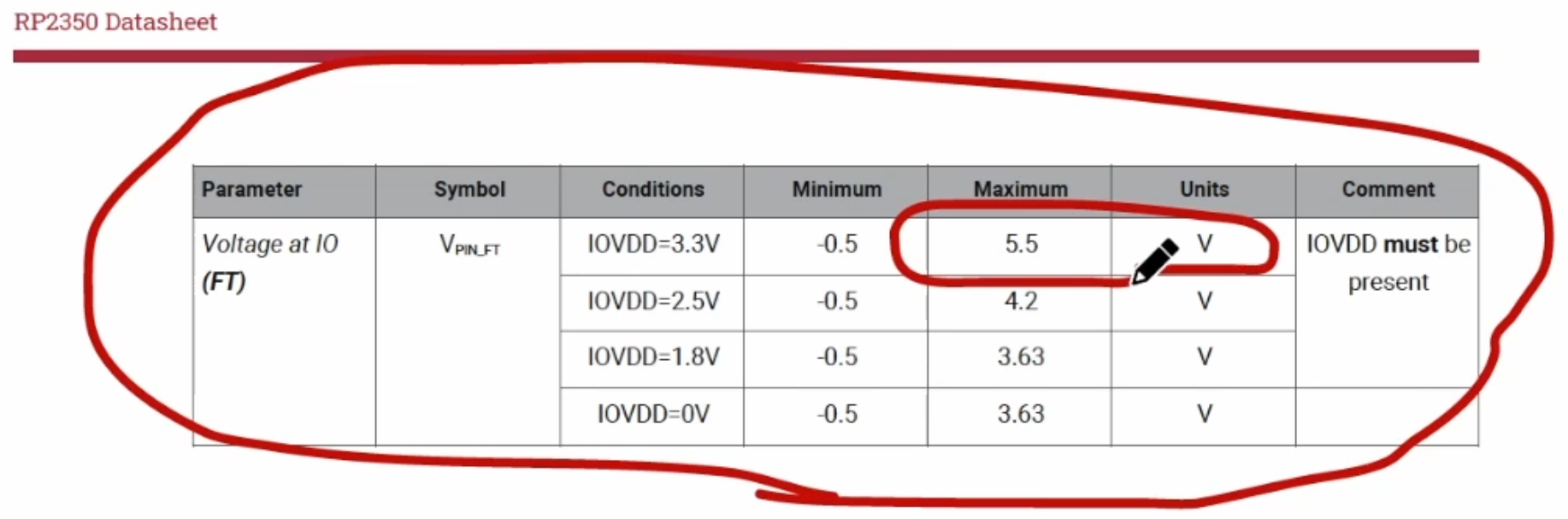
5V Tolerance
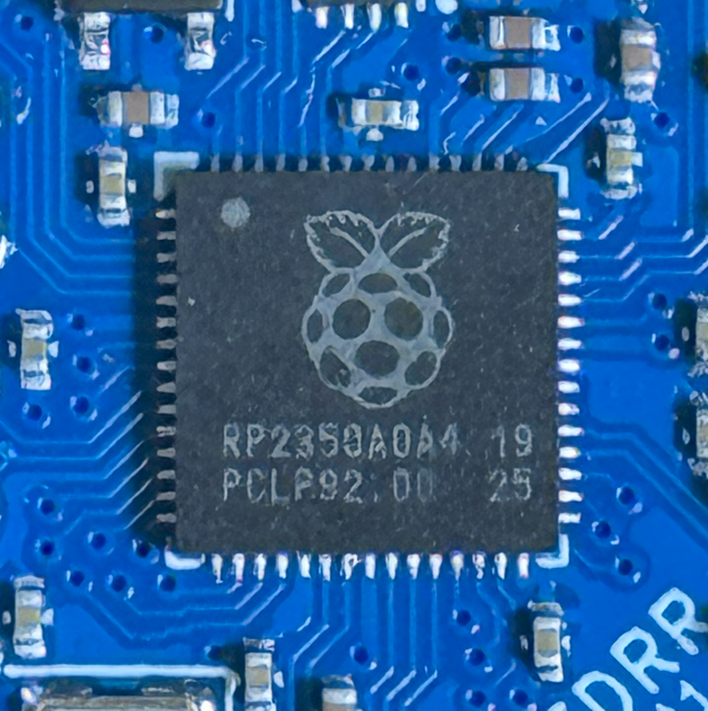
Much has been made of the new RP2350’s newly qualified 5V tolerant GPIOs. This is true for GPIOs 0-25, but not for the ADCs - GPIOs 26-29. One ROM therefore uses pins 0-23 to connect to the host.
Also, the input/output high/low voltage thresholds in the datasheet do seem to be compatible with the retro chips One ROM is used with (6502, VIC-II chip, etc).
But beware. The RP2350 has an absolute maximum voltage on any pin of 5.5V. The original Commodore chips tended to tolerant up to 7V, at least according to their datasheets. This is likely to be the case for other types of retro systems. The STM32F4 is tolerant up to an absolute maximum voltage of 7.3V. If you have a retro machine with a suspect voltage regulator or power supply, you are likely to be taking a risk using an RP2350 in it.
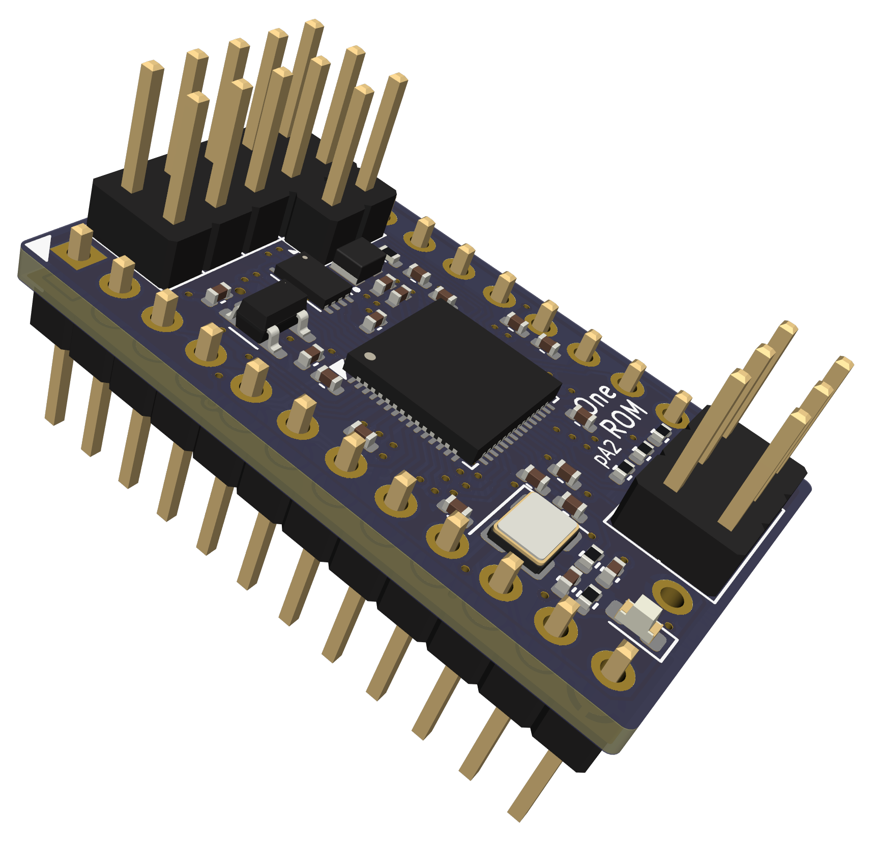
Space Constraints and Layout
Due to the physical form factor of the ROMs being replaced by One ROM, and other design choices (the desire to have image select jumpers, the same programming header as the STM version, and only have components on a single side to keep manufacturing cost low), the entire area of the PCB available for the RP2350, plus supporting componentry, is roughly 17mm x 14mm. A thumbnail if you have slightly bigger thumbnails than me. Or around 1/3 sq inch.
While the RP2350 itself is only 7mm x 7mm, I had to include:
- A voltage regulator (as per the STM32 boards, the AP2112K).
- External flash (it is internal on the STM32s).
- External crystal oscillator (it is internal and reasonably good on the STM32s - the internal oscillator on the RP2350 is, frankly, crap, and only good - and probably only intended for - getting the chip to start up).
- External decoupling and voltage regulator capacitors (similar to the STM32 boards, but more of them are recommended).
- A polarised (!) inductor for the internal voltage regulator (not required on the STM32).
- Status LED, resistor and a few pull-ups (per the STM32 boards).
This is around 30 surface mount components in total. The 7x7mm RP2350 and the 3.2x2.5mm crystal are starting to look mighty large at this point.
As with the STM32 boards it was a design goal to avoid going below 0402 sized components, to make hand-assembly at least possible (not necessarily easy), and to be able to use the cheapest PCB assembly services.
At this point you might be thinking “sure, but the STM32 package you use on those boards is huge so surely that was tought to route around”. Yes, it is large - 14mm x 14mm. But, and it is a very big but, you can route traces directly underneath it as it has no ground pad.
Much of the underside of the RP2350 is a solid ground pad, with any remaining space taken up by the 2 required power voltages. In addition, you’re supposed to have stitching vias through the entire ground pad, primarily to help with heat dissipation, but also to provide a good ground return path for things like the external voltage regulator circuitry.
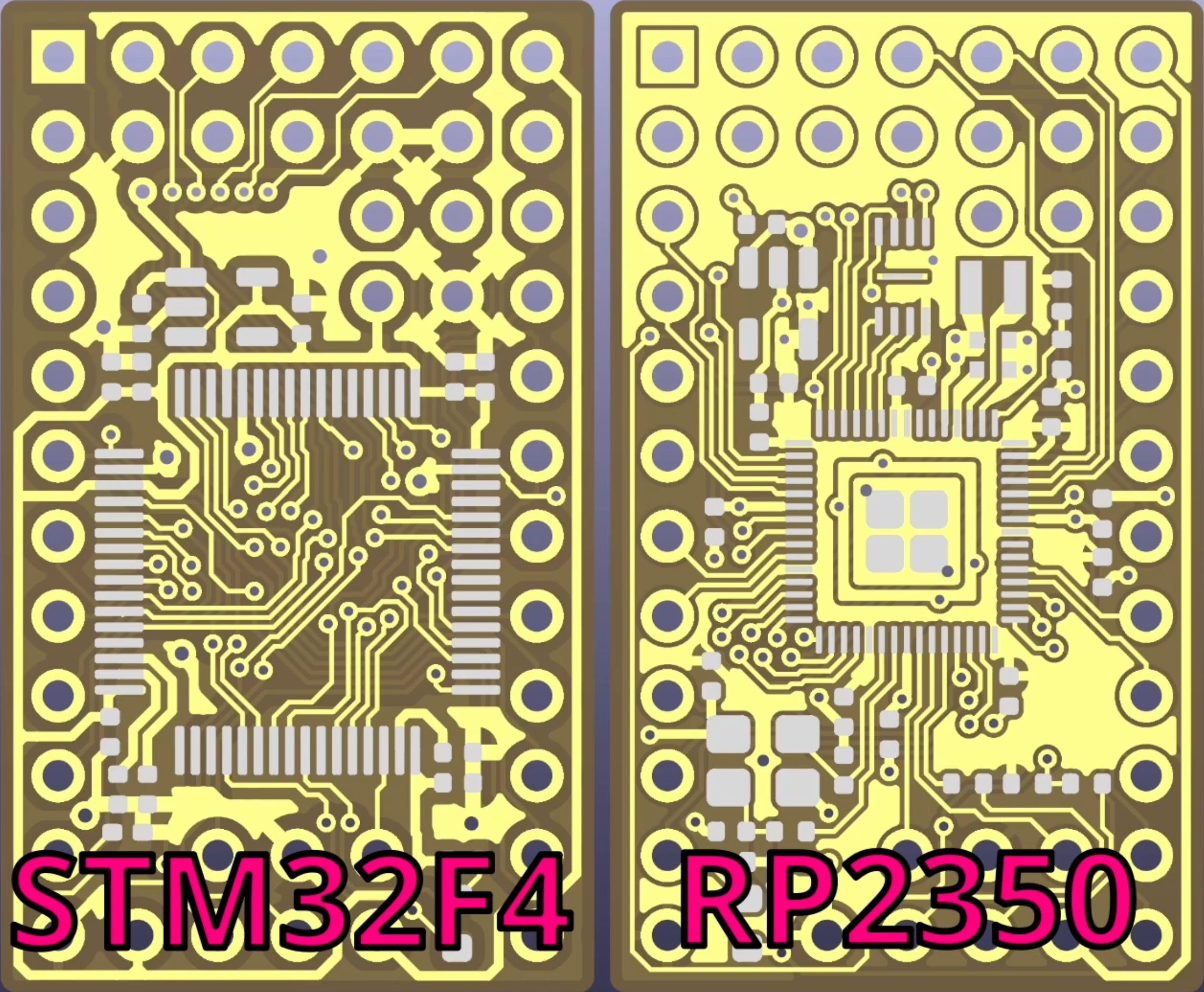
This would mean that you also can’t route traces on the underside of the PCB either, under the RP2350. This might then push you, not to a 4-layer board (gains you very little in this case), but to a 6-layer board (expensive). And/or to very fine traces. But the 6 mils (6/1000ths of an inch) I used tends to be the minimum side supported by the cheapest PCB fab services.
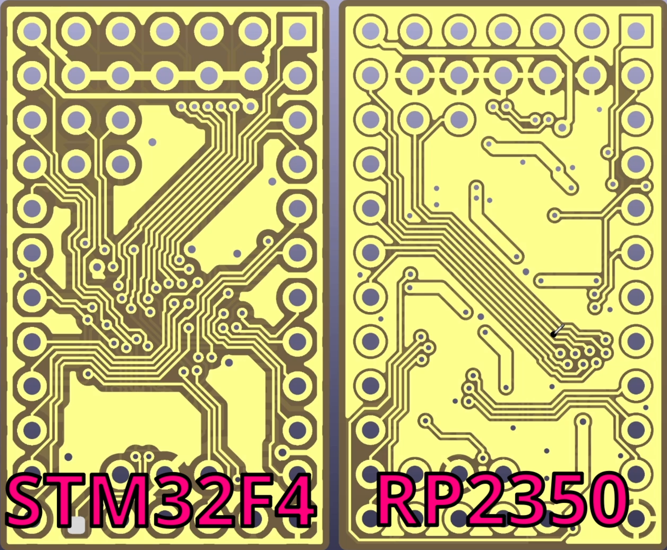
In the end, with some creative pin assignments (that still allow One ROM’s highly optimised assembly code to be very similar to the STM32 version), very few stitching vias, and a lot of careful routing, I managed to fit everything in. But just barely. In hardware revision A, only 3 image select jumpers are exposed, compared to the STM32F4’s 5 - although there are 2 more unused GPIOs just waiting to be used. By the time you read this, there may be a further revisions with more jumpers exposed - I have an idea that might just allow me to get them routed.
Power On
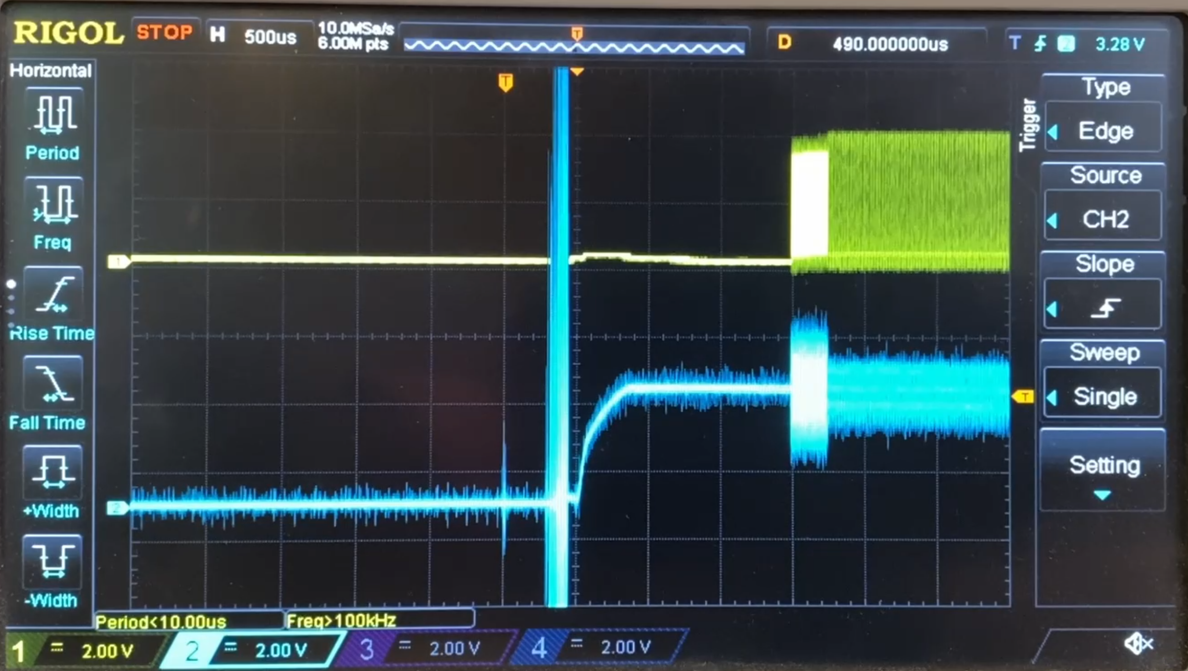
I measured power on delay using an oscilloscope, measuring the time from 3.3V becoming available on the chip, until the main loop started executing. I know when the main loop has started execting by measuring GPIO 26 which drives One ROM’s status LED - it is pulled low at the start of the loop execution (and, in fact, due to one of my software optimisations, shows bytes being served which is fun!).
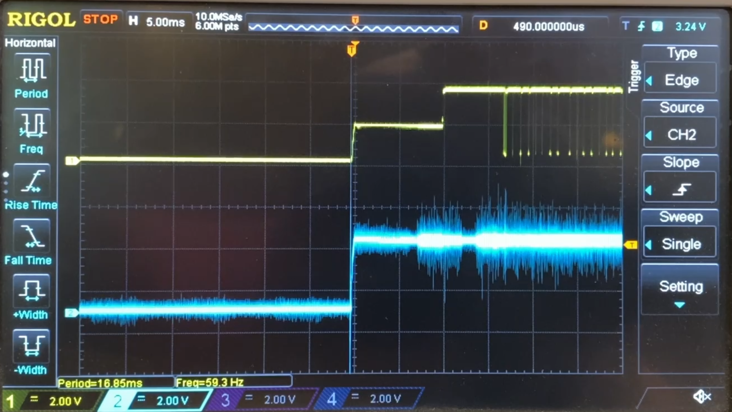
I see:
- GPIO 26 go mid-level (~1.8V) at power on, and stay there for 10ms.
- GPIO 26 go high (3.3V) at that point and stay there for 8ms in “normal” operation, with One ROM’s debug logging enabled.
- GPIO 26 then goes low and starts showing bytes being served.
By removing logging and ROM image preload to RAM I can reduce the GPIO 26 high period to 6ms.
This suggests 10ms for the chip to come out of reset, 5ms for the ROM bootloader to start One ROM’s code, and 1-3ms for the code to get to the main loop (depending on build options).
There are unlikely to be major gains possible here. It may be possible to speed up One ROM’s preloading the ROM image to RAM (which is necessary - serving from ROM would be too slow), by using DMA instead of a memcpy, but it’s only going to save around a millisecond at the most.
The STM32F4, in the same application takes under 2ms (1.5ms in testing) from power on to main_loop execution. That’s an order of magnitude faster.
Overclocking
There are a number of considerations when overclocking the RP2350.
PLL Settings
Simply, the on-board PLL takes the clock source (external crystal in this case), and takes it through an number of multipliers and dividers to generate the system clock.
The Pico SDK tool vcocalc.py is very useful for calculating the settings required, although One ROM generates its own PLL settings based on the frequency requested at build time.
Flash Speed
The appropriate flash access timing must be set using the QMI M0_TIMING register. The flash chosen for revision A is the W25Q16JV, which has a maximum clock speed of 133MHz. When clocking the RP2350 beyond this speed, the system clock needs to be divided down for flash access. A divider of 3 is actually the RP2350’s default, but One ROM is more aggressive, and sets it lower if it can according to the target MCU frequency.
Regulator Voltage
The stock voltage regulator voltage is 1.1V, which, from testing, is good to drive the RP2350 up to around 300MHz. Beyond that, the voltage needs to be increased. 420MHz was possible with 1.3V, but was probably right on the edge. Frequencies beyond that need higher voltages, which in turn requires unlocking voltage limits within the RP2350. 540MHz at 1.6V was the highest I was prepared to go, and One ROM faithfully served a C64 character ROM at this speed.
Your mileage is likely to vary, depending on the exact silicon you have, temperature, application, cosmic particles, etc.
Temperature
Running faster, means more power, means more heat. One ROM’s first RP2350 PCB has only 2 stitching vias from the RP2350 GND pad to the underside, as opposed to 9 in the reference design, so its ability to dissipate heat is limited. If overclocking you would be wise to install a small heat-sink on the RP2350, to monitor temperature, and perhaps expect premature failure of the RP2350.
The RP2350 has an internal temperature sensor, which can be read using the ADC peripheral. When overlocking beyond 300MHz is enabled, One ROM enables the ADC and temperature sensor, and reads it and logs it before entering its main loop. You could continue to read this periodically - which would be more useful than detecting the temperature before it starts working hard! - either via an external SWD device, or with code running on the second core (which would generate more heat…).
Programming
One ROM has no USB connection, so therefore an SWD Debug Probe like Raspberry Pi’s Debug Probe is used to program it.
During development I mostly used Rust-based probe-rs to program the RP2350, while it was installed in a host (a long-suffering Commodore 64).
I found that I had to put the RP2350 into BOOTSEL mode (pulling BOOT low and resetting), in order to program it each time. This is a bit of a pain, as you have to short a cable from the PCB’s USB_BOOT to GND, and then power cycle the board. You know when One ROM’s in BOOTSEL mode, as the status LED will glow faintly - presmably due to the RP2350 leaving GPIO 26 in an uninitialized state while starting up.
I suspect this programming issue is due to probe-rs not fully resetting the RP2350 before programming it, rather than an RP2350 specific problem. If I tried to re-program the RP2350 without pulling in BOOTSEL mode, the first re-flash appeared to work - but hadn’t really. A second time hard-failed.
The same behaviour was observed with a Pico 2 (W), so I don’t believe this is a problem with the One ROM PCB.
Speed vs STM32
To get the obvious comparisions out of the way first:
| RP2350 | STM32F4 | |
|---|---|---|
| Max Speed | 150MHz | 84-180MHz |
| Cortex | M33 | M4 |
| Cores | 2 | 1 |
| Flash | External | Internal |
| RAM | 520KB | 64-192KB |
The code between the STM32F4 and RP2350 variants of One ROMs is very, very similar, and in particular, at the time of writing, the assembly main byte serving loop is essentially identical. You would therefore naively expect the performance to be the same, Hz for Hz between the two devices, as they are both ARM Cortex cores, running the same assembly, at the same speed.
However, this is not the case.
But first, what do I mean by performance? I mean One ROM serving bytes to the host system, so it behaves correctly and does not crash. If one MCU can serve a C64 character ROM without visual glitches or host crashes, at 80MHz, but another needs 100MHz, I consider the latter to be slower, and might be very loose and say it’s 20% slower, or the other 20% faster. Yes, my stats teacher would be horrified. I never liked stats. But it’s all approximate anyway so try not to get too angry with me.
Minimum clock speeds required:
| RP2350 | STM32F4 | |
|---|---|---|
| C64 char ROM | 80Mhz | 80MHz |
| C64 kernal ROM | 90MHz | 84MHz |
Why do I think there is any difference? Two key reasons:
- Flash, in particular, instruction cache.
- RAM and bus architecture.
Flash
The STM32F4xxR series has an ART Accelerator. I won’t get into the gory details here, but for One ROM it appears to cause the device to behave as if the device has zero flash wait states. This is a good thing.
There are also some differences between STM32F4 models here - the F405’s ART Accelerator appears worse than the other, later models, such as the F401, F411 and F446. So let’s forget about the F405 for now. The ART Accelerator for the others is great, a least for One ROM. There appears to be zero touching of flash from within One ROM’s main loop, and I can erase and re-program One ROM’s flash while the main loop is running, without any problems.
The RP2350 on the other hand has a quite difference flash architecture. For one thing, flash is external using QSPI, and for another the RP2350 has an XIP (eXecute In Place) cache instead of the ART Accelerator. I don’t fully understand it (see XIP Cache Pinning later!), but it is a different approach to caching.
In One ROM I attempt to “warm” the XIP cache by reading the main_loop() function from flash, immediately before executing it. Maybe this helps, I’m not sure. But I suspect it isn’t as good as the STM32’s ART Accelerator for this application and hence I think there may be more variability in performance Hz for Hz. And perhaps the C64’s 6510 processor is more sensitive to timings than the VIC-II is - hence replacing the kernal ROM requires a slightly faster clock speed than the character ROM. I’m speculating.
RAM and Bus Architecture
Like the flash, I think the RAM and bus matrix architecture is a bit different between the two MCUs, although there’s not that many details in the RP2350 datasheet on this topic.
I therefore think that the RP2350 may involve a bit more jitter while running due to bus contention than the STM32. Having said this, I am currently loading bytes to be served via RAM, and accessing GPIOs via the SIO, which probably is using the same bus matrix and probably introducing contention.
I might be able to reduce contention by using PIOs to serve bytes (it has direct GPIO connection). However, using the direct GPIO Coprocessor (GPIOC) is slower when compared to SIO access.
I did upload the ROM image to be served to a dedicated SRAM bank to try and reduce contention. Maybe that helped?
GPIO Coprocessor
What is the GPIO Coprocessor (GPIOC)? Cortex M33 (on which the RP2350 is based), has a concept of co-processors, which are directly connected to the core, and can be accessed using ARM-v8m instructions, such as MCR. This approach is described in the RP2350 datasheet 3.6.1 GPIO Coprocessor (GPIOC).
There are two primary benefits touted of this approach:
- You bypass the bus matrix, and therefore avoid bus contention.
- You can operate on the entire 48 GPIOs in a single instruction. The RP2350A only has 30 GPIOs, so this is irrelevant.
I tested using MCR instructions to set the data lines to outputs/inputs (when the ROM chip select goes active/inactive) and found worse performance when using GPIOC compared with SIO. Specifically, for serving the C64 character ROM stably, I needed to at 80MHz using GPIOC, vs 78MHz using SIO.
(Yes, this figure of 78MHz conflicts with the 80MHz given earlier - it was a different day, and such variations happen.)
I speculate one or both of two reasons for this:
- XIP instruction cache impact. The MCR instructions are 32-bit wide, rather than the STR instructions I use in the SIO case. I struggle to believe this as the cause, as this approach only introduces 4 more bytes into the very compact main loop.
- The GPIO Coprocessor is simply not as optimised as the memory-mapped GPIO and bus access.
I have not really found anything online discussing this approach, either using the RP2350, or other ARM Cortex processors. It is possible that any benefit would be more apparent in a different use case, for example when using the second core for heavy memory access.
I have not attempted to use GPIOC to read the address lines, or to apply values to the data lines, as my current approach will always be faster - it requires no masking or bit shifting as a result of some cunning PCB and assembly optimisations. A GPIOC approach would require shifting/masking (an extra cycle) in both cases.
XIP Cache Pinning
Reading the RP2350 datasheet, in particular 4.4. External Flash and PSRAM (XIP), I concluded that I could “pin” certain flash addresses to the XIP cache, in order to ensure the main_loop() was already loaded into the XIP cache, and would be executed from there - to avoid any wait states if the CPU had to load instructions from flash. Even a single wait state during the first iteration of the main loop and therefore failing to serve the first byte quite within the necessary time can crash the ROM’s host.
I tried this pinning - by reading the main_loop() function from flash, and then pinning it to the XIP cache.
I tried pinning jut “way” 0, and pinning both “ways”.
However, this either caused a core lock-up (when pinning both ways and then continuing), or a fault (pinning way 0 then continuing). I don’t know why, but suspect I have misunderstood the XIP cache, and it’s really intended for use with external PSRAM instead.
SIO Sub-word Writes, and Reads
The RP2350’s single-cycle IO (SIO) subsystem is, as it sounds, used to perform single-cycle reads and writes to GPIOs. All of the SIO registers are 32-bit wide, and registers are provided to modify individual or arbitrary sets of bits with single-cycle (atomic) operations.
Buried in the detail elsewhere in the datasheet, in 2.1.5 Narrow IO Register Writes is the statement:
“[Memory-mapped IO registers] treat all writes as though they were 32 bits in size. This means software cannot use byte or halfword writes to modify part of an IO register: any write to an address where the 30 address MSBs match the register address affects the contents of the entire register.”
This suggests that one cannot safely write an 8-bit or 16-bit value to an SIO register. This can be done on other MCUs. This limitation is fine for many use cases - just mask/shift your bits and use the registers that operate on that desired set of bits. But in the One ROM use case, every cycle counts. Reading on:
“Upon a 8-bit or 16-bit write (such as a strb instruction on the Cortex-M33), the narrow value is replicated multiple times across the 32-bit data bus, so that it is broadcast to all 8-bit or 16-bit segments of the destination register”
Aha, this is very useful. In One ROM we read a single byte from RAM and want to apply it to 8 data lines, GPIOs 16-23. This means we can write the byte (8-bits) we have just retrieved from RAM to the SIO’s GPIO OUT register, and the hardware will replicate it across the entire 32-bit register, and apply it to GPIOs 16-23 - avoiding a shift operation, saving a cycle. As we don’t have any other GPIOs in output mode, this is a safe operation, and we don’t mind having the other GPIO outputs set with the same byte.
The is no similar limitation on reads - we can read an 8-bit or 16-bit value from an SIO register without problems. This is also useful in One ROM, as we have the address and CS lines as GPIOs (0-15), allowing us to read the entire address and CS state with a single ldrh (half-word load) instruction. This is then used as an offset to a RAM array containing the bytes to be served. Again, no shift or mask is required, saving a cycle.
Erratum E9
Erratum E9 affects the RP2350 A2 stepping and essentially prevents the use of RP2350’s internal pull-ups/pull-downs, requiring external pulls (where pulls are required).
One ROM makes use of internal MCU pulls, both for its image select jumpers (which are read at boot time to select a ROM image), and at run-time (to allow dynamic switching between images and also serving multiple ROM sockets simultaneously from a single ROM). External pulls are avoided due to board space issues - there simply isn’t space for the 5x0402s that would be required for external pull.
I can report that One ROM’s image/bank/rom switching function operates as designed, so although I haven’t explicitly tests the internal pulls, they do appear to be operating as expected.
It Verks
This is what most surprised me, and much as I thought ill of them during PCB layout, the Raspberry Pi engineers have done a cracking job of Hardware design with RP2350. I read it and re-read it repeatedly during design and layout, and BOM selection, and followed it as closely as possible - and I was rewarded by One ROM’s RP2350 design working first time.
Ship it!
Conclusion
What are my takeaways?
Although I remain a bit nervous of the RP2350’s absolute maximum voltage on any pin of 5.5V (as I’ve seen some of my systems hit 5.5V), now I am past the pain of the fscking board layout, I think the RP2350 gives an overall better solution than the STM32F4:
- It is roughly the same price or cheaper in quantity.
- It can be laid out on a the PCB in the same space as alternatives.
- It is roughly as performant (within 10%) at the same clock speed.
- It can be overclocked higher.
- It has more flash, more RAM, a second core, and those PIOs.
- It’s British.
Well done Raspberry Pi.
comments powered by Disqus